
The Post-Moore Path for AI Chips: Advanced Packaging Succeeds Process Scaling
For decades, the semiconductor industry rode a remarkably simple storyline: shrink transistors, pack more of them onto a die, and enjoy automatic gains in performance and efficiency. That story—embodied in Moore’s Law—still matters, but for AI chips in the mid‑2020s it is no longer the sole, or even primary, driver of progress.
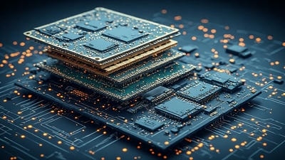
This blog explores how advanced packaging has become the new frontier for AI chips, why it now often matters more than pure process scaling, what technologies define this packaging revolution, and how this shift reshapes design, manufacturing, and system‑level thinking in the AI era.
Why process scaling alone is no longer enough
Node shrinks once delivered a predictable trifecta for logic chips: more transistors, higher frequencies, and lower power per operation. For AI workloads, that formula ran into limits. Modern AI accelerators already pack billions of transistors, and raw frequency increases hit diminishing returns due to power density and thermal constraints. Meanwhile, memory bandwidth and data movement emerged as primary bottlenecks.
At the most advanced nodes, shrinking further yields benefits but at enormous cost. Mask sets, design complexity, and yield challenges escalate. Certain structures—especially memory—do not scale as gracefully as logic, and interconnect delays begin to dominate. For AI chips whose performance depends heavily on feeding massive arrays of compute units, simply squeezing more transistors onto a single die cannot fully solve bandwidth and efficiency problems.
In this context, the industry has turned increasingly to advanced packaging: techniques that orchestrate multiple dies, memory stacks, and interconnect fabrics within a single package to deliver system‑level improvements that process scaling alone cannot achieve.
The rise of chiplets: breaking the monolithic die

A central element of the post Moore path is the shift from monolithic dies to chiplet‑based designs. Instead of building one giant chip that contains all functionality, designers split systems into multiple smaller dies—compute tiles, memory stacks, I/O complexes—and integrate them in a package using advanced interconnects.
This chiplet approach offers several advantages. Smaller dies improve yield, reducing the impact of defects. Different chiplets can be manufactured on different process nodes: bleeding‑edge logic for compute, mature nodes for analog or I/O, specialized processes for memory. Designers gain flexibility in composing systems without forcing every function onto the most expensive node.
For AI chips, chiplets allow vendors to scale out compute and memory capacity horizontally using packaging as the scaling vehicle. Performance improvements come from adding or rearranging chiplets and improving their connections, rather than exclusively from shrinking transistors.
In effect, chiplets turn the package into a modular canvas, where the architecture of the AI system is defined across multiple dies rather than constrained to the footprint of a single monolithic chip.
2.5D and 3D integration: moving into the vertical dimension
Advanced packaging goes beyond placing multiple dies side by side. 2.5D and 3D integration introduce vertical and near‑vertical dimensions to chip construction, stacking or closely coupling logic and memory to reduce distance and improve bandwidth.
In 2.5D schemes, logic dies and memory stacks sit on a silicon interposer or advanced substrate that provides high‑density interconnect between them. This enables very wide, short connections—ideal for AI workloads where massive parallel data transfer between compute units and memory is essential.
3D integration takes this further by stacking dies directly, using through‑silicon vias or other vertical interconnects. Memory can sit atop logic or be integrated in tiers, shortening paths and potentially reducing energy per bit moved.
For AI accelerators, these approaches are transformative. Instead of treating memory as a distant resource, advanced packaging pulls it physically closer, enabling architectures where compute and memory interact more like parts of a single layered system than separate components. The gains in effective bandwidth and latency come from geometry and integration, not just transistor size.
CoWoS, InFO, and other advanced packaging platforms

Several specific advanced packaging platforms have become central to AI chips. While details vary by vendor and foundry, they share themes: high‑density interconnect, support for multi‑die assemblies, and integration of high‑bandwidth memory.
One widely discussed platform is chip‑on‑wafer‑on‑substrate (CoWoS), which connects large logic dies with multiple high‑bandwidth memory stacks on a shared interposer. This arrangement delivers extremely wide memory interfaces and dense wiring between compute and memory, enabling AI accelerators to reach bandwidth levels that would be impossible with traditional board‑level connections.
Other platforms, such as fan‑out wafer‑level or panel‑level packaging, provide high‑density routing without a traditional organic substrate, improving signal integrity and potentially reducing form factor. These are used in certain AI and high‑performance systems to combine multiple dies in compact, efficient packages.
What matters for the post Moore path is that these packaging platforms are now treated as primary design spaces. Engineers optimize how chips use them just as intensely as they once optimized transistor layouts, because packaging choices often determine the real‑world performance and efficiency of AI systems.
High‑bandwidth memory and the end of memory starvation
AI workloads are notoriously memory‑hungry. Large models and training batches require moving immense amounts of data between compute units and memory. Early AI accelerators often found themselves starved by conventional memory architectures, regardless of how powerful their cores were.
Advanced packaging, particularly with integrated high‑bandwidth memory (HBM), has changed that picture. HBM stacks mounted near logic dies via interposers or other advanced packaging techniques provide wide buses and high aggregate bandwidth with relatively low power per bit. AI chips can now access tens or hundreds of gigabytes per second per stack, multiplied across multiple stacks per package.
The impact is profound. Instead of being constrained by narrow, off‑package memory links, accelerators can sustain data flows that more closely match their compute capability. Training and inference run more efficiently, with fewer stalls and lower energy overhead for memory access.
Critically, these advances in memory bandwidth come from packaging more than from process scaling. HBM structures themselves may sit on different process nodes, but their performance advantage arises from how they are placed and connected relative to logic. This exemplifies how advanced packaging succeeds process scaling as the primary tool for unlocking AI performance.
Die‑to‑die interconnect: turning packages into mini‑systems

As chiplet and multi‑die designs proliferate, die‑to‑die interconnect within packages becomes a central design concern. Rather than relying on board‑level interfaces with long traces and higher power, advanced packaging enables short‑reach, dense links between dies, turning packages into tightly coupled mini‑systems.
Die‑to‑die interconnect technologies aim to deliver high bandwidth, low latency, and low energy per bit across millimeter‑scale distances. They often use parallel “bunch of wires” approaches or standardized fabrics tailored for in‑package communication. Their performance characteristics shape how chiplets can be composed: whether compute tiles and memory tiles can behave as near‑neighbors or must treat each other more like external devices.
For AI chips, strong die‑to‑die interconnect allows designers to split functionality across multiple dies without suffering major penalties at the boundaries. Compute clusters, cache tiles, memory controllers, and specialized accelerators can be distributed in the package while still interacting at speeds close to on‑die fabrics.
This in‑package system‑building is a hallmark of the post Moore path: the package becomes the new “board,” and die‑to‑die links become the new “internal bus,” enabling complex AI systems to be assembled from modular components without relying solely on process shrinks for performance.
Advanced packaging and power: efficiency from geometry
Beyond pure performance, advanced packaging influences power efficiency. Moving data over long board traces and through multiple layers of I/O circuits consumes substantial energy. By shrinking distances and simplifying interfaces, advanced packaging reduces the power cost of data movement—a critical factor in power‑hungry AI clusters.
Shorter connections between logic and memory, enabled by interposers and stacked structures, require less voltage swing and fewer equalization stages. In‑package links avoid some of the heavy signaling overhead associated with off‑package interconnect. As a result, energy per bit transferred can drop, improving overall system efficiency.
For AI chips operating at high utilization, these savings accumulate. Power budgets constrained by cooling and infrastructure limits benefit from packaging decisions that cut energy spent on moving data rather than on computing. In many cases, geometry and integration—the domain of advanced packaging—offer more room for power optimization than further shrinking transistors.
This reinforces the idea that the post Moore path is not only about doing more; it is about doing more with less, by reorganizing how and where computation and memory physically reside.
Design philosophy shifts: architects think in packages, not just dies
As advanced packaging rises in importance, chip architects change how they think about design. The package becomes an integral part of the architecture, not merely a container. Decisions about core counts, memory capacity, and interconnect topology are made in tandem with packaging choices.
Architects now consider questions such as: How many chiplets per package? How should HBM stacks be arranged relative to logic tiles? What die‑to‑die bandwidth is required to keep compute units fed? How does thermal management interact with vertical stacking?
These design questions blur the line between traditional “front‑end” and “back‑end” chip engineering. System architects must collaborate closely with packaging experts and process technologists to ensure that concepts are physically realizable and efficient.
For AI chips, where system‑level behavior—training throughput, inference latency, cluster power—is the ultimate metric, this package‑centric design philosophy is essential. It marks a shift away from viewing scaling as purely a process‑node story and toward viewing scaling as a holistic integration challenge.
Manufacturing and supply chain: packaging as a new bottleneck
The success of advanced packaging brings new manufacturing and supply chain challenges. Where process nodes once dominated capacity planning, packaging lines and substrate supply now represent critical constraints, particularly for complex AI packages with multiple HBM stacks and large interposers.
Scaling advanced packaging capacity involves specialized equipment, trained labor, and refined processes. Yield issues can arise not only at the die level but also in assembly: misalignment, interposer defects, and thermal stress can impact package‑level output. Supply of substrates, interposers, and memory components must be coordinated with logic production.
These factors make packaging capacity a strategic resource. AI chip vendors and their manufacturing partners must plan packaging investments as carefully as logic fabs. In some cycles, packaging rather than process may become the bottleneck that limits how many AI chips can ship.
This supply chain reality underscores the extent to which advanced packaging has succeeded process scaling as a first‑class concern: the ability to package complex AI systems at scale is now as important as fabricating the underlying dies.
Implications for AI system and data‑center design
The rise of advanced packaging also affects how AI systems and data centers are designed. When packages contain more tightly integrated compute‑memory complexes, system architects adjust cluster topologies, node configurations, and deployment strategies.
Nodes built around advanced‑packaged AI chips may offer higher performance per slot, higher memory capacity per accelerator, and different balance between local compute and network bandwidth. This can lead to fewer nodes for a given workload or new strategies for distributing models across accelerators and memory resources.
Network fabric design must align with the capabilities of packaged AI chips, ensuring that inter‑node bandwidth complements the high intra‑package bandwidth. Cooling and power infrastructure must accommodate packages with dense, stacked structures and high power density, but potentially fewer external interfaces.
In short, advanced packaging radiates outward: it reshapes not only chip design, but also how AI clusters are built and how data centers plan their AI deployments, reinforcing its status as a central pillar of the post Moore path.
Conclusion: advanced packaging as the new engine of AI chip progress
The phrase “post Moore” does not imply that process scaling has ended; it signifies that node shrinks are no longer the sole or dominant engine of performance gains for AI chips. Advanced packaging—chiplets, 2.5D and 3D integration, high‑bandwidth memory, dense die‑to‑die interconnect—has stepped into that role, enabling system‑level advances that process alone cannot deliver.
As AI workloads grow in complexity and scale, the success of future accelerators will hinge on how effectively they exploit these packaging technologies. Architects, manufacturers, and system designers must treat packaging as a core strategic domain, not a secondary afterthought. In doing so, they trace the new path of progress for AI hardware: one where integrating, arranging, and connecting silicon succeeds simply shrinking it, and where the package becomes the true canvas on which AI performance is drawn.





